


The recent conclusion of Semicon India 2026 has brought the nation’s technological ambitions into sharp focus. The event underscored a period of unprecedented momentum; with twelve major projects—ranging from a landmark silicon fabrication unit to compound fabs and advanced packaging facilities—now approved under the India Semiconductor Mission, the country has secured a formidable investment pipeline exceeding ₹1.64 lakh crore. Yet, amidst the justifiable celebrations of India’s rapidly expanding semiconductor footprint, a troubling and entirely predictable narrative has emerged in certain digital quarters.
Scrolling through platforms like X, one can easily stumble upon comments—such as this dismissive thread—scoffing at India’s strategic investments in semiconductor packaging and testing. The comments were made in reaction to the presentation of chips made in India during Semicon 2. Social media users asked why ‘mere’ testing and assembling a chip is considered a huge achievement, when we don’t have a fabrication unit in the country. These critics have argued that the official celebration of “chips made in India’s semiconductor plants” overstates what is actually happening on the ground, with the claim that ‘packaging and testing’ of chips is not part of actual manufacturing.
For these social media semiconductor experts, chip making means the actual fabrication of chips on wafers, and the later steps of packaging and testing are not so important, and there is nothing to celebrate in India’s achievements in the process. In these arguments, the underlying assumption is that “testing” means plugging a chip into a simple multimeter, and “packaging” is merely wrapping it in a piece of plastic or a cardboard box before shipping. But in reality, this is an entirely mistaken assumption, and the processes of packaging and testing of chip are not what they sound like.
This misunderstanding of the semiconductor value chain is not a new phenomenon; it is a familiar symptom of a cynical mindset that habitually underplays India’s industrial milestones. We witnessed this exact same dismissive chorus just a few years ago during the early days of the mobile phone manufacturing push. At the time, critics gleefully mocked the nascent factories as mere “screwdriver technology” or “just assembly plants,” arguing that piecing together imported parts held little true economic value.

However, industrial history offers a consistent lesson: nations establish deep component ecosystems only after they anchor down high-volume manufacturing. That initial phase of final assembly was precisely what was required to create massive economies of scale. Today, as a direct consequence of that scale, India’s mobile manufacturing sector has organically evolved. We are now seeing substantial investments in high-value component manufacturing—including battery packs, camera modules, complex printed circuit board (PCB) assemblies, and display enclosures—rapidly taking root on Indian soil. As a result, smartphones have quietly surged to become the nation’s single largest export product. This progression from downstream assembly to upstream component fabrication is the natural, time-tested trajectory of global industrialisation.
Now, as India embarks on its most ambitious deep-tech push to date, the cynics have simply changed their target from mobile phones to microchips, completely ignoring the mind-boggling complexity of modern electronics. The process of making a chip is a highly integrated, technologically formidable triad: Design, Fabrication, and Assembly & Test. The process of assembling and testing a chip is not some mundane process; it is actually one of the three most important steps in modern semiconductor manufacturing.

To truly appreciate why India’s strategic investments across this entire spectrum are revolutionary rather than rudimentary, one must delve deep into what these three monumental steps actually entail.
When we think of the world’s most powerful technological behemoths—companies synonymous with the artificial intelligence revolution, gaming, and high-performance computing—names like NVIDIA and Advanced Micro Devices (AMD) instantly spring to mind. These giants dictate the pace of global innovation. Yet, it is a fascinating paradox of the modern tech industry that neither NVIDIA nor AMD actually manufactures the physical chips they sell. They are what the industry calls “fabless” semiconductor companies.
Several other major tech giants, including Qualcomm, Broadcom, MediaTek, Realtek, etc., do not make their chips; they only design them. They outsource the actual manufacturing to semiconductor giants like TSMC, the Taiwanese multinational semiconductor contract manufacturing company. Their entire empire is built on the very first, incredibly complex pillar of the chipmaking process: Design, and it does not involve any factory. The fabrication units work like traditional contract manufacturing units; they produce chips as per the design specifications of the chip designer.
Companies that design and fabricate their own chips include Intel, Samsung, Micron, Texas Instruments, SK Hynix, etc. They are known as integrated device manufacturers.
Semiconductor design is the intellectual bedrock of the entire industry. It is the process of deciding exactly what a chip will do and meticulously planning how billions of microscopic transistors will be arranged to achieve that function. Modern chips, such as those powering generative AI or flagship smartphones, contain upwards of 50 billion to 100 billion transistors squeezed onto a piece of silicon no larger than a fingernail. Designing this is akin to drawing a flawless roadmap for a city the size of the Earth, where a single dead-end street could cause the entire global logic system to crash.
To truly comprehend why the semiconductor design phase is a monumental feat of modern engineering—and why fabless giants like NVIDIA and AMD command trillion-dollar valuations without owning a single factory—one must peel back the layers of how a microchip is actually conceived. Semiconductor design is not merely sketching a schematic; it is the intellectual bedrock of the entire industry. It involves translating an abstract mathematical concept into a physical blueprint containing up to 100 billion microscopic transistors, where a single misplaced connection can cause a multi-million-dollar production batch to fail.
This mind-boggling process is executed through a rigorously structured pipeline, seamlessly blending high-level software programming with extreme physics:

The journey begins at the conceptual level, akin to urban planners deciding the fundamental purpose of a new mega-city. Architects and system engineers define exactly what the chip needs to achieve. Will it be a Central Processing Unit (CPU) for a laptop, a Graphics Processing Unit (GPU) for rendering video games, or a specialised Neural Processing Unit (NPU) dedicated entirely to crunching artificial intelligence algorithms. During this phase, engineers establish the chip’s Instruction Set Architecture (ISA)—such as ARM or x86—and define strict budgets for power consumption, thermal limits, and processing speed.
Once the architecture is locked in, the conceptual blueprint must be translated into digital logic. Remarkably, modern chips are initially written entirely in code. Hardware engineers utilise specialised programming languages known as Hardware Description Languages (HDL), such as Verilog or VHDL, to write the RTL code. This code dictates exactly how data will flow between the microscopic registers of the chip with every tick of the system clock. It is, essentially, software that describes the behaviour of physical hardware.
Before a single physical transistor is mapped out, the RTL code undergoes the most arduous and time-consuming stage of the entire design cycle: Verification. In fact, up to 70% of a design team’s time and resources are poured into this single phase. Engineers build incredibly complex virtual simulations to stress-test the code, throwing billions of randomised scenarios at the digital model to ensure it behaves flawlessly. If a logical bug slips past this stage and makes it onto the physical silicon, it cannot be fixed with a simple software patch over the internet; the physical chip is permanently ruined.
Once the RTL code is verified to be logically perfect, it is fed into highly advanced Electronic Design Automation (EDA) software. This synthesis tool automatically translates the lines of code into a “gate-level netlist”—a colossal, sprawling schematic of foundational logic gates (AND, OR, NOT, NAND) that will perform the actual computations.

This is where the abstract logic finally takes a physical shape. Using immensely powerful EDA tools from global leaders like Synopsys and Cadence, engineers must now figure out how to physically arrange these billions of logic gates onto a tiny sliver of silicon no larger than a fingernail. This stage has three components:
Floorplanning: Engineers divide the silicon canvas into distinct blocks, deciding where the memory caches will sit and where the processing cores will reside, much like zoning commercial and residential districts in a city.
Placement: The software algorithms calculate the optimal placement for every single transistor to minimise the distance signals need to travel.
Routing: This is arguably the most complex geometrical puzzle ever solved by humanity. The software must draw the microscopic, multi-layered copper wiring that connects the billions of transistors. Engineers must perform exhaustive timing analyses to ensure that an electrical signal travelling across the chip arrives at its exact destination within fractions of a nanosecond, without suffering from signal interference, voltage drops, or thermal hotspots.
In the final stage, the completed physical layout undergoes severe Design Rule Checking (DRC) to ensure it complies with the extreme physical limitations of the fabrication plant’s photolithography machines. Engineers also perform Layout Versus Schematic (LVS) checks to confirm the physical drawing perfectly matches the original logic netlist. Once thoroughly validated, the multi-layered blueprint is compiled into an industry-standard master file format known as GDSII. This file is then securely transmitted to the foundry—a momentous milestone known in the industry as “tape-out.”
The process of chip design is an exercise in extreme optimisation—engineers must balance power consumption, thermal limits, and processing speed, ensuring that electrical signals can travel across the chip without interference or delay.
Crucially, India does not need to start from scratch in this domain; we are already a global powerhouse. While the world may only now be noticing India’s manufacturing push, global tech giants have relied on Indian engineering brilliance for decades. Today, approximately 20% of the world’s Very-Large-Scale Integration (VLSI) design workforce sits in India. Massive research and development centres operated by Intel, AMD, Qualcomm, NVIDIA, and Texas Instruments are spread across Bengaluru, Hyderabad, Noida, and Pune.
The chips powering your laptop, your smartphone, and even the servers running your favourite cloud applications likely have significant portions of their logic designed by engineers sitting in India. Through the government’s Design Linked Incentive (DLI) scheme, the focus is now shifting from providing talent for global MNCs to nurturing indigenous fabless startups that will design and own proprietary intellectual property (IP), creating the Indian NVIDIAs and AMDs of tomorrow.
Recognising that producing world-class microchips requires a formidable pipeline of talent equipped with the right technological instruments, the Indian government has initiated a sweeping democratisation of semiconductor education through its landmark Chips to Start-up (C2S) Programme. Historically, the astronomical licensing costs of industry-standard Electronic Design Automation (EDA) software created a massive barrier to entry for most universities, restricting practical chip design to a privileged few. To dismantle this bottleneck, the Ministry of Electronics and Information Technology (MeitY) established the ChipIN Centre at C-DAC Bengaluru, which acts as a centralised national hub. The government has absorbed the multi-million-dollar costs to procure licenses from global EDA titans like Cadence, Synopsys, and Siemens, providing unfettered, cloud-based access to over 400 academic institutions, spanning premier IITs to engineering colleges in Tier-II and Tier-III cities.
Crucially, the initiative goes far beyond mere virtual simulations. Through an ingenious system of Multi-Project Wafers (MPW), the ChipIN Centre aggregates the most promising student-designed circuits and sends them for physical fabrication at the Semi-Conductor Laboratory (SCL) in Mohali. This extraordinary initiative allows engineering students to not only master complex digital blueprints but to actually hold their conceptual innovations as functional, physical silicon chips. By bridging the gap between theoretical classroom learning and high-end industrial execution, the government is systematically forging an immense, industry-ready workforce poised to drive India’s homegrown fabless revolution.
Once the chip designers complete the architectural blueprint, the baton is passed to the foundries. This brings us to the second pillar: Fabrication, or “Fab.” If design is the architecture, fabrication is the construction. But this is construction operating at the absolute extremes of human capability, manipulating materials at the atomic level. Semiconductor fabrication plants are some of the most expensive and complex facilities ever built by mankind, often costing upwards of $15 billion to $20 billion to construct.

The process begins with a blank canvas: a wafer of pure silicon, extracted from ordinary sand but purified to a staggering 99.9999999% perfection. Inside a “cleanroom,” which is tens of thousands of times cleaner than a hospital operating theatre to prevent a single speck of dust from ruining a nanoscale transistor, this wafer undergoes a relentless, month-long cycle of physical and chemical transformations. The wafer is coated with light-sensitive materials, baked, bombarded with ions, and etched with highly reactive gases in a cyclic process that repeats hundreds of times to build the chip layer by layer.
At the very heart of this modern alchemy is a process called photolithography, which is the incredibly precise foundational process at the heart of semiconductor fabrication, effectively acting as a nanoscale printing press that transfers complex architectural blueprints onto silicon wafers. The meticulous procedure begins by coating a hyper-purified silicon wafer with a light-sensitive chemical compound known as a photoresist. Inside a sterile cleanroom environment, ultraviolet light, and in the most advanced nodes, Extreme Ultraviolet (EUV) light, is projected through a photomask containing the chip’s intricate master design. When this high-energy light strikes the wafer, it fundamentally alters the chemical structure of the exposed photoresist, allowing those specific microscopic regions to be dissolved and washed away by a developer solution. This creates a temporary, sub-microscopic stencil on the wafer, exposing the bare silicon underneath to subsequent stages of chemical etching or ion implantation; a cyclic marvel that is repeated dozens of times to layer and build the billions of nanometre-scale transistors that power our modern digital world.

The necessity for Extreme Ultraviolet (EUV) lithography for advanced chips stems directly from the fundamental physical limits of light and the relentless demands of Moore’s Law. For decades, the semiconductor industry relied upon Deep Ultraviolet (DUV) lithography, using light with a wavelength of 193 nanometres to print transistor patterns. However, as the insatiable drive for more powerful and energy-efficient chips pushed transistor architectures down to the 7-nanometre threshold and beyond, DUV light simply became too “thick” to accurately draw such microscopic features—akin to attempting to draft a precise architectural blueprint using a broad paintbrush. To breach this physical barrier, the industry mandated the leap to EUV light, which boasts an incredibly short wavelength of just 13.5 nanometres. This ultra-fine wavelength acts as a nanoscale scalpel, permitting foundries to etch exponentially smaller, denser, and more intricate circuit patterns onto the silicon wafer without the debilitating blurring and diffraction issues that cripple older optical systems. Ultimately, without the deployment of these immensely complex EUV machines, the fabrication of the advanced, high-density chips that currently propel artificial intelligence, 5G telecommunications, and high-performance computing would remain physically impossible.
This domain of Extreme Ultraviolet lithography is effectively ruled by a single, undisputed monarch: a Dutch company named ASML. To create transistors that are just a few nanometres wide (a strand of human hair is roughly 100,000 nanometres thick), foundries require ASML’s Extreme Ultraviolet (EUV) lithography machines. The technology inside these machines borders on science fiction. To generate EUV light, the machine fires a high-powered laser at microscopic droplets of molten tin falling through a vacuum chamber, hitting each droplet twice—once to flatten it and a second time to vaporise it into plasma. This happens 50,000 times per second d. The resulting ultra-short wavelength light is collected by the flattest mirrors ever created by humanity and projected through a reticle (the stencil of the chip design) to print impossibly tiny patterns onto the silicon wafer.
Among the most critical, yet commonly overlooked, components of a semiconductor fabrication plant is ultra-pure water (UPW). Because the fabrication process involves hundreds of sequential chemical baths, reactive etching cycles, and photolithography steps, the delicate silicon wafer must be aggressively washed after almost every single operation to prevent chemical cross-contamination. However, ordinary purified water is woefully inadequate for this job. UPW is filtered to such an extreme degree that all minerals, dissolved gases, ions, and particulates are entirely stripped away, creating an unnaturally pure solvent. At the nanometre scale of modern transistors, a solitary rogue sodium ion or a microscopic speck of organic matter left behind by a water droplet can act as a massive boulder, fatally short-circuiting the logic gates. Consequently, a single commercial fab consumes millions of litres of this hyper-refined liquid every single day, further underscoring the staggering infrastructural and chemical complexity required simply to keep the silicon clean.
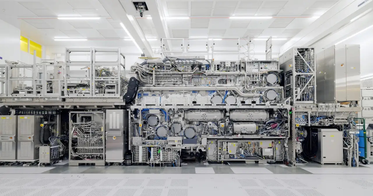
The fabrication step is unforgiving. A slight variance in temperature, chemical concentration, or vibration can render an entire batch of wafers useless. Until recently, India was entirely absent from this segment of the value chain. However, a monumental shift is underway. With the foundation of the Tata Electronics fabrication plant in Dholera, Gujarat, in partnership with Taiwan’s Powerchip Semiconductor Manufacturing Corporation (PSMC), India is taking its first giant leap into commercial chip fabrication. While this fab will initially target mature nodes (28nm and above) essential for automotive, power electronics, and telecommunications, it represents a watershed moment, building the deeply complex supply chain of specialty gases, ultra-pure water, and highly trained metallurgical and chemical engineers required to keep a fab running.
This brings us to the final, and currently most debated, stage of the manufacturing process: Assembly, Testing, Marking, and Packaging (ATMP), also broadly referred to as Outsourced Semiconductor Assembly and Test (OSAT). While the process involves ‘packaging’, it must be understood that it does not mean packaging in a conventional form; it is not the process of putting chips in plastic boxes. It is the final step where the chips fabricated on wafers are tested and given the final form of usable semiconductor chips. Advanced packaging has become the most critical bottleneck and the hottest battleground in modern technology because of its complexity.
When a finished silicon wafer emerges from the fabrication plant, it is essentially a fragile, easily destructible piece of glass containing hundreds of tiny, individual chips known as “dies.” A naked die cannot simply be plugged into a motherboard. It requires a highly engineered interface to communicate with the motherboard, receive power, and, most importantly, dissipate the immense heat it generates. This is what packaging achieves.
Before the fragile silicon wafer is even sliced into individual pieces, it must undergo a brutal and fascinating process known as wafer sort or probe testing. At this stage, the wafer contains hundreds of naked dies, but due to the microscopic imperfections inherent in atomic-level chemical fabrication, not all of them will function flawlessly. To prevent wasting highly expensive advanced packaging on “dead” silicon, foundries must identify the “Known Good Dies” (KGD). This is achieved using highly specialised automated test equipment equipped with a probe card—a device resembling a microscopic hairbrush containing thousands of ultra-fine tungsten or beryllium-copper needles. These needles meticulously make physical contact with the microscopic pads on each individual die across the uncut wafer, injecting electrical signals to rigorously evaluate logic functions, memory arrays, and power efficiency before the diamond saws ever touch the silicon.

Crucially, this testing is not merely a binary pass-or-fail exercise; it is the foundation of a highly lucrative and deeply practical industry strategy known as silicon binning. Consider the ubiquitous Intel Core processors that power millions of computers globally. When Intel fabricates a new generation of desktop chips, they do not necessarily design entirely separate architectural blueprints and fabrication masks for the Core i3, i5, i7, and flagship i9 models. Instead, they aim to manufacture the top-tier, fully unlocked Core i9. During the initial wafer probe testing, if a specific die proves to be a flawless “silicon lottery” winner—capable of sustaining the highest clock speeds across all its cores without overheating or leaking power—it earns the prestigious i9 badge.
But what if a die has minor manufacturing defects in two of its eight cores, or if it runs slightly too hot to hit the peak frequencies? Instead of discarding this immensely valuable silicon, Intel simply uses microscopic lasers to permanently disable the defective parts and electronically limit the maximum clock speeds. The chip is then strategically rebranded and packaged as a Core i7 or an i5 depending on the level of fault. If even more cores are defective, it is binned further down as a budget-friendly Core i3. This ingenious testing and categorisation strategy maximises the usable yield from every multi-million-dollar wafer, allowing manufacturers to drastically reduce waste while simultaneously catering to diverse consumer price points from a single physical production line.
While some fabrication units do this testing and binning in-house, most units send the untested wafers to Assembly and Test units where this process is done before the process of packaging starts.
Modern chip packaging involves incredibly complex metallurgy, thermal dynamics, and materials science. Once the probe testing has successfully identified the “Known Good Dies” and categorised them according to the level of fault, the fragile silicon wafer moves into the Assembly and Packaging phase. This is the moment the naked silicon is transformed into a robust, deployable electronic component. To the untrained eye, this final product might look like a simple piece of black plastic, but it is, in reality, a heavily engineered micro-environment constructed from highly specialised materials.

The assembly process is a meticulously orchestrated sequence of operations:
The process begins by cutting the circular wafer into individual, rectangular chips. This is not achieved with standard blades. Foundries employ ultra-precision dicing saws impregnated with microscopic diamond grit, spinning at upwards of 30,000 to 60,000 revolutions per minute. For the thinnest and most advanced wafers, laser ablation is used to vaporise the silicon along designated “street” lines. During mechanical sawing, continuous streams of ultra-pure deionised water are aggressively sprayed over the wafer to cool the intense friction and wash away microscopic silicon dust that could short-circuit the transistors.

Once separated, a robotic vacuum arm gently picks up the individual die and mounts it onto a base, known as a lead frame or a substrate. Securing the die requires far more than standard industrial adhesives. Engineers utilise specialised die attach pastes or films. These are typically complex thermosetting epoxy resins that are heavily loaded with microscopic silver flakes. The silver is crucial; it provides excellent thermal and electrical conductivity, ensuring that the immense heat generated by the billions of computing transistors is rapidly drawn away from the silicon and transferred to the heatsink.
A chip mounted on a substrate is useless until it can communicate. Highly reliable “wire bonding” is used for this process, where capillary machines stitch microscopic wires between the die’s contact pads and the substrate. These wires—thinner than a human hair—are forged from ultra-pure gold, copper, or aluminium. However, for modern, high-performance chips (like CPUs and AI processors), the industry uses a technique called “flip-chip.” Instead of wires, microscopic solder bumps (usually a lead-free tin-silver-copper alloy) are electroplated directly onto the face of the die. The die is then flipped upside down and aligned with matching pads on the substrate. The entire assembly is heated in a reflow oven, melting the solder to create thousands of incredibly short, high-speed electrical pathways.

The substrate itself is a marvel, acting as a structural and electrical bridge between the microscopic chip and the macroscopic computer motherboard. Because the chip’s wiring is so unfathomably dense, the substrate must be built using multiple, staggering layers of copper circuitry to fan out the signals. These copper layers must be perfectly electrically isolated from one another. Herein lies one of the most fascinating anomalies in the history of the tech industry. The critical insulating material that separates these microscopic copper layers was not invented by a traditional tech giant, but by Ajinomoto, the Japanese food and chemical corporation globally famous for manufacturing MSG (Monosodium Glutamate) seasoning.

In the late 1990s, their researchers repurposed their expertise in amino acid chemistry to create a thermosetting resin film. This product, known as Ajinomoto Build-up Film (ABF), offered unprecedented electrical insulation and thermal resistance, and was perfect for laser-drilling microscopic vias (holes). Today, the entire global supply chain of high-performance computing—virtually every advanced PC, gaming console, and AI server—relies completely on this “seasoning company’s” insulating film to function.
Finally, the delicate, interconnected assembly must be shielded from moisture, oxygen, dust, and physical trauma. The substrate and die are placed inside a steel mould cavity, and a molten Epoxy Moulding Compound (EMC) is injected under high pressure. The EMC is a deeply sophisticated chemical cocktail. It consists of epoxy resins meticulously blended with spherical fused silica (glass) fillers. The addition of silica is absolutely critical; it alters the coefficient of thermal expansion of the plastic to precisely match that of the silicon die. If this ratio is even slightly off, the intense heat cycles of the chip turning on and off would cause the plastic to expand at a different rate than the silicon, literally ripping the chip’s microscopic wiring apart from the inside.
Thus, the journey from a bare wafer to a packaged chip is an exhaustive gauntlet of materials science, chemistry, and extreme precision engineering—a far cry from simply putting a chip in a box. Furthermore, as Moore’s Law (the historical trend of shrinking transistors) begins to hit the hard limits of physics, the industry has pivoted to “Advanced Packaging” or “Heterogeneous Integration.” Instead of trying to fabricate one massive, flawless chip, companies now manufacture smaller, modular chips called “chiplets” and use advanced packaging to stitch them together side-by-side or stack them vertically in 3D structures using Through-Silicon Vias (TSVs). This microscopic architectural marvel allows memory and processing units to sit fractions of a millimetre apart, enabling the immense data transfer speeds required for modern AI servers. Without advanced packaging, the AI revolution currently sweeping the globe would immediately grind to a halt.
Once the delicate silicon die is securely encapsulated within its protective resin housing, the manufacturing process is still far from complete. To assume that a fully packaged chip is simply tossed into a shipping crate after a cursory power check is perhaps the most egregious misunderstanding of the semiconductor lifecycle. Instead, the newly minted microchip enters the most punishing and demanding stage of its existence: post-assembly testing.
This phase is not about gently confirming if the device turns on. It is an aggressive, highly orchestrated interrogation designed to push the silicon to its absolute breaking point, ensuring that only the most robust chips make it into global supply chains. This rigorous post-assembly evaluation is broadly categorised into three distinct, highly specialised phases: Final Test, Burn-In, and System-Level Testing.
The journey begins with the Final Test (FT), a procedure executed by multimillion-dollar mainframes known as Automated Test Equipment (ATE). This market is effectively a global duopoly dominated by two engineering giants: Teradyne from the United States and Advantest from Japan.
An ATE system is not a glorified multimeter; it is a hyperspeed supercomputer explicitly designed to interrogate other computers. When a packaged chip—such as a modern smartphone System-on-Chip (SoC) featuring over 2,000 microscopic connection pins—is inserted into the ATE’s test socket, the machine simultaneously connects to every single pin. Over the course of mere seconds, the ATE bombards the chip with millions of “test vectors” (complex sequences of electrical signals).
The ATE demands responses with unimaginably strict parameters. It measures voltage accuracy down to fractions of a millivolt and timing accuracy to within a few picoseconds (a picosecond is one-trillionth of a second). During this phase, the chip undergoes structural testing, utilising built-in self-test (BIST) circuitry to verify that billions of microscopic copper interconnects within the chip are not short-circuited or severed. This is followed by functional testing, where the ATE simulates the exact high-speed digital environments the chip will experience in the real world. If a single transistor out of 50 billion misfires by a fraction of a nanosecond, the ATE instantly flags the entire package as defective.
Even if a chip flawlessly passes the Final Test, semiconductor physics dictates a cruel reality: latent defects. Due to microscopic anomalies in the atomic structure of the silicon or the packaging metallurgy, a certain percentage of chips are destined to fail within their first few months of operation—a phenomenon the industry calls “infant mortality”.
To prevent these infant mortalities from occurring inside a consumer’s laptop, an autonomous vehicle, or a critical hospital ventilator, manufacturers utilise Burn-In Testing. This is a deliberate, highly calculated method of accelerated artificial aging.
Thousands of freshly packaged chips are loaded onto specialised printed circuit boards and inserted into massive thermal chambers or “burn-in ovens.” The environment inside these ovens is hostile. The chips are subjected to extreme thermal stress, typically baked at 125°C to 150°C, whilst simultaneously being injected with operating voltages significantly higher than their designated limits.
The chips are forced to actively run intense computational cycles in this inferno for anywhere from 24 to 168 continuous hours. The underlying physics relies on the Arrhenius equation, which dictates that elevated temperatures exponentially accelerate chemical and physical degradation. A week inside a burn-in oven effectively simulates a year of heavy real-world usage. By intentionally stressing the dielectric layers and metal pathways, the factories force any structurally weak chips to completely fail in the laboratory, ensuring that the surviving batch possesses the ironclad reliability required for mission-critical applications.
Historically, ATE and Burn-In were sufficient to guarantee a chip’s viability. However, in the era of artificial intelligence and radically complex heterogeneous packaging—where multiple chiplets are stacked together in 3D—the testing paradigm has evolved to include a final, exhaustive hurdle: System-Level Testing (SLT).
While an ATE machine is brilliant at firing synthetic electrical vectors at a chip, it struggles to replicate the chaotic, unpredictable environment of a fully functioning computer system. Therefore, SLT takes the fully packaged chip and places it onto a bespoke motherboard that flawlessly mimics its final destination environment.
Instead of synthetic test vectors, the SLT rig actually boots up a full commercial operating system, such as Windows or Linux, directly off the chip. It then runs authentic, heavy software workloads: playing high-definition video files, rendering complex 3D graphics, or executing massive neural network AI models. SLT is designed to hunt down the most elusive “corner-case” bugs—glitches that only manifest when the CPU, the memory controller, and the power management unit are all simultaneously stressed by messy, real-world software code.
By the time a semiconductor component successfully navigates the picosecond-precision of ATE, survives the thermal purgatory of Burn-In, and boots an operating system during System-Level Test, it has proven itself to be one of the most rigorously validated manufactured objects on the planet.
Therefore, to dismiss this multi-stage, highly advanced scientific interrogation as simple testing is a spectacular failure to comprehend the sheer scale of engineering required to keep the modern digital economy alive.

The often-overlooked ‘M’ in ATMP, Marking, serves as the vital cryptographic link for the entire global supply chain. Once the delicate silicon is securely packaged within its hardened epoxy moulding compound, the blank plastic canvas must be branded with its definitive identity before it can be shipped out to the world.
This is far from a simple stamping exercise. The marking process meticulously engraves critical metadata onto the chip’s surface, including the manufacturer’s logo, the precise part number, the date of manufacture, the batch or lot code, and increasingly, complex 2D data matrix barcodes. Historically, this was achieved using specialised inks, but modern ATMP facilities rely almost exclusively on high-speed laser marking systems. These precision lasers ablate the surface of the epoxy resin at microscopic depths, altering the chemical composition of the plastic just enough to create a stark, permanent visual contrast without generating excess heat or vibration that could damage the fragile die inside.
This step is crucial for traceability and security. If a critical component unexpectedly fails in a commercial airliner, a medical ventilator, or an autonomous vehicle, the laser-etched markings allow engineers to trace that exact chip back through the labyrinthine global supply chain. It allows them to identify not only the specific ATMP facility that packaged it, but the exact fabrication plant, the specific silicon wafer, and the very hour it was manufactured. Furthermore, in an era where counterfeit electronics pose a multi-billion-dollar threat to national defence and consumer safety, sophisticated laser marking acts as a formidable first line of defence, ensuring the unassailable authenticity and provenance of the silicon driving our digital economy.
Recognising that ATMP is a highly sophisticated, high-value, and deeply essential part of the semiconductor ecosystem, India has strategically aggressively pursued this segment. The Micron ATMP facility in Sanand, Gujarat, the massive Tata Electronics OSAT facility in Morigaon, Assam, and the CG Power joint venture in Gujarat are not mere “boxing” factories. They are highly automated, cleanroom-based technological fortresses. Establishing these plants builds the foundational culture of extreme precision manufacturing in India. It creates the ecosystem of logistics, chemical suppliers, and equipment technicians that the broader semiconductor industry requires.
Therefore, mocking ATMP as a low-level chore is to profoundly misunderstand how semiconductor technology works. Design, Fabrication, and Packaging are not a hierarchy of importance, but a tightly woven, interdependent trinity. You can design a brilliant chip, and you can fabricate it with cutting-edge EUV lithography, but without the microscopic marvels of advanced packaging and the unforgiving rigour of sophisticated testing, that chip will never power a server, steer a car, or boot up a smartphone. By planting its flag firmly in all three domains, India is not skipping steps or settling for the easiest tasks; it is methodically building an end-to-end ecosystem that will secure its technological sovereignty for generations to come.
The undeniable success of India’s initial foray into the chipmaking space—Semicon 1.0—laid a formidable groundwork. With twelve manufacturing units approved, drawing a cumulative investment of over ₹1.64 lakh crore, the nation proved its serious intent to global players. The fact that facilities operated by Micron, Kaynes, and CG Semi have already commenced commercial production underscores a rapid transition from policy to physical output. However, establishing isolated fabrication and packaging units is simply not enough to secure true technological sovereignty. Recognising this, the Union Cabinet in July 2026 took a decisive leap, approving the monumental Semicon 2.0 programme with a staggering budget outlay of ₹1,27,500 crore.
If the first phase was about planting the flag, Semicon 2.0 is about fortifying the entire fortress. The government has strategically broadened its vision far beyond just Assembly, Testing, Marking, and Packaging (ATMP) and mature node fabrication. Semicon 2.0 is meticulously designed around six comprehensive pillars aimed at indigenising the entire supply chain and mitigating the risks of global over-reliance.
Firstly, the focus on Design is being significantly deepened. Having already empowered over 105 startups to begin chip development, Semicon 2.0 shifts the objective towards generating indigenous Intellectual Property (IP). The goal is not merely to provide brilliant engineering talent to global tech giants, but to ensure that the core architectures of future compute, memory, and radio frequency systems are owned and developed by Indian entities.
Secondly, and perhaps most critically for long-term sustainability, is the introduction of a pillar dedicated exclusively to Machines and Materials. Semiconductor fabrication requires ultra-pure chemicals, specialised gases, and precision machinery that are incredibly difficult to source. Under the new scheme, companies setting up Research and Development (R&D) or manufacturing for these vital raw inputs will receive substantial incentives. This is a vital step toward creating a truly self-reliant precision manufacturing industry, ensuring that a future disruption in the global supply of speciality chemicals does not throttle Indian foundries.
Furthermore, Semicon 2.0 aggressively pursues the establishment of more Fabs and Advanced R&D. While the nation’s first major silicon fab at Dholera is slated for commissioning in 2028, the new policy specifically targets the development of more advanced computing nodes. Moving beyond the mature 28nm-110nm spectrum, India is now facilitating collaborations with premier global R&D centres to master next-generation technologies. This broader technological portfolio is complemented by recent approvals under the India Semiconductor Mission, such as the CRYSTAL MATRIX integrated compound semiconductor fab in Dholera and SUCHI SEMICON’s new OSAT facility in Surat, pushing the nation into high-value silicon carbide and gallium nitride domains.
Finally, knowing that human capital is the ultimate differentiator, the programme scales up Talent Development. Having already trained around 68,000 students across 315 universities on complex Electronic Design Automation (EDA) tools, the next phase will aggressively deepen the level of engineering training at the university level.
Ultimately, this ₹1.27 lakh crore investment is a bold declaration that India is no longer content with being just a participant in the global semiconductor supply chain. By simultaneously nurturing raw material ecosystems, expanding ATMP capacities, and funding advanced IP design, Semicon 2.0 is engineering a robust, end-to-end semiconductor powerhouse on Indian soil.

While India achieves its E20 ethanol blending target, vehicle compatibility disputes and food-security concerns persist. Synthetic drop-in fuels—produced via coal gasification, biomass hydropyrolysis, methanol, ethanol, or captured CO₂—offer chemically identical alternatives that run in existing engines without blending or modifications.

From recent sugarcane controversies to the cutting edge of synthetic biology, discover why ethanol is a non-negotiable pillar of India’s energy security and how 1G, 2G, 3G, and 4G ethanol technologies actually work.

From extreme orographic cloudbursts to thawing permafrost triggering massive rock-ice avalanches, the ‘Third Pole’ is facing an unprecedented ecological emergency. This deep dive explores the thermodynamic, geological, and human forces making the Himalayas increasingly dangerous.


